 We just pushed up the v2.1 hardware designs to the git server. You can find instructions for ordering PCBs and a zip file containing all of the KiCAD, and gerber files on the wiki.
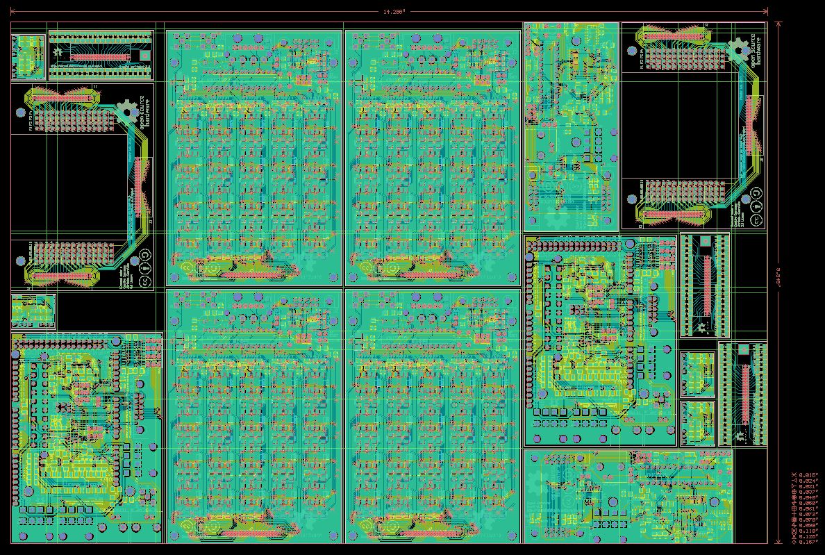
This new design is a minor update to the v2.0 series. The biggest changes are:
- The new high-voltage switching boards are 2-layer (previously they were 4-layer). This means that they are cheaper to fabricate and can now be ordered on a single panel with the rest of the PCBs.
- The new high-voltage switching boards have their own microcontroller. Previously they used a general purpose input output (GPIO) chip, which was one of the most difficult chips in the system to solder because it was so tiny! In the future, having a microcontroller on these boards will make it possible to add new functionality.
- All surface mount capacitors/resistors now have a minimum size of 1206 (previously, some of the capacitors were much smaller and more difficult to solder manually).
- All of the boards now have hardware support for in-system programming (meaning that in the future, it will be possible to flash the firmware for all of the microcontrollers over a single USB cable automatically).
If you have any questions/comments, post them to the dev list. If anyone gets boards assembled using the stencil reference numbers, let us know; we’re curious to see how that works out.
7 Comments